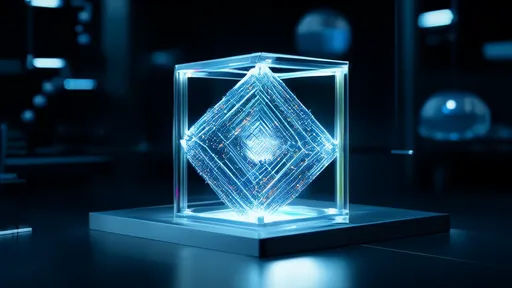
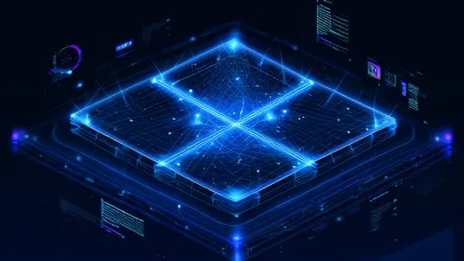
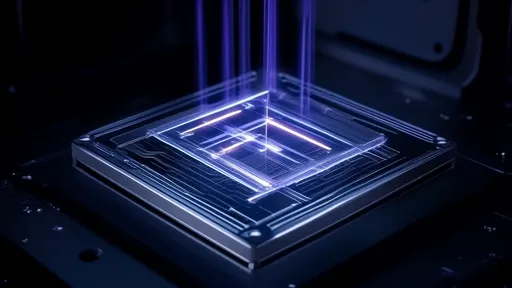
The realm of photonic crystals has long fascinated scientists and engineers alike, offering unprecedented control over light propagation. Among the myriad fabrication techniques, femtosecond laser weaving has emerged as a groundbreaking approach to constructing three-dimensional photonic crystals with intricate architectures. This method harnesses the precision of ultrafast lasers to sculpt materials at the nanoscale, enabling the creation of structures that were once confined to theoretical models.
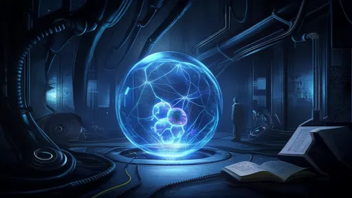
At the heart of this innovation lies the ability of femtosecond lasers to induce nonlinear absorption in transparent materials. Unlike conventional lasers, these ultrafast pulses deposit energy so rapidly that they bypass thermal diffusion, allowing for sub-micron precision. When applied to materials like glass or polymers, the laser can selectively modify refractive indices or even create voids, effectively "weaving" a three-dimensional photonic lattice. The result is a crystal that can manipulate light in ways previously unimaginable.
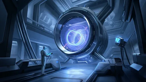
The implications of this technology are profound. Photonic crystals engineered through femtosecond laser weaving exhibit unique optical properties, such as complete photonic bandgaps. These bandgaps prevent certain wavelengths of light from propagating through the crystal, analogous to how electronic bandgaps in semiconductors control electron flow. Such capabilities open doors to advanced optical devices, from ultra-efficient waveguides to sensors with unparalleled sensitivity.
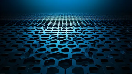
One of the most striking advantages of this technique is its versatility. Traditional methods for creating photonic crystals often rely on complex lithographic processes or self-assembly, which can be limiting in terms of design flexibility. Femtosecond laser weaving, by contrast, is a direct-write approach. This means that researchers can tailor the photonic crystal's structure on-the-fly, adjusting parameters like lattice symmetry, unit cell size, and defect placement with remarkable precision. The ability to introduce controlled defects is particularly valuable, as these imperfections can be engineered to create localized states for light, enabling functionalities like optical trapping or enhanced light-matter interactions.
Recent breakthroughs have pushed the boundaries of what's possible with this technique. Scientists have demonstrated the fabrication of woodpile structures, gyroid lattices, and even quasi-crystalline arrangements—all with feature sizes smaller than the wavelength of visible light. These complex geometries are not just academic curiosities; they enable novel optical phenomena such as negative refraction or superprism effects, where light bends in counterintuitive directions. Such properties are invaluable for developing compact photonic circuits or cloaking devices.
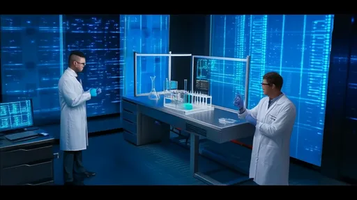
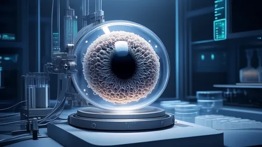
The marriage of femtosecond lasers with advanced materials has further expanded the horizons of this field. By doping glasses with rare-earth ions or incorporating quantum dots into polymers, researchers can create active photonic crystals that not only guide light but also emit or modulate it. This convergence of structural control and functional materials paves the way for integrated photonic systems that could revolutionize telecommunications, quantum computing, and biomedical imaging.
Despite these advancements, challenges remain in scaling up production and improving fabrication speeds. Current femtosecond laser systems, while precise, are relatively slow for industrial-scale manufacturing. However, emerging techniques like parallel processing with spatial light modulators or the use of high-repetition-rate lasers show promise in addressing these limitations. As these technologies mature, we may soon see photonic crystals woven by femtosecond lasers transition from lab curiosities to commercial components.
Looking ahead, the potential applications seem boundless. Imagine optical computers where information is processed at the speed of light with minimal energy loss, or biomedical implants that use photonic crystals to precisely deliver light therapy to damaged tissues. The ability to construct three-dimensional photonic environments with femtosecond precision brings us closer to turning these visions into reality. As researchers continue to refine laser weaving techniques and explore new material combinations, the future of photonic crystal engineering appears brighter than ever.
By /Aug 5, 2025
By /Aug 5, 2025
By /Aug 5, 2025
By /Aug 5, 2025

By /Aug 5, 2025
By /Aug 5, 2025
By /Aug 5, 2025
By /Aug 5, 2025

By /Aug 5, 2025
By /Aug 5, 2025

By /Aug 5, 2025

By /Aug 5, 2025

By /Aug 5, 2025
By /Aug 5, 2025
By /Aug 5, 2025

By /Aug 5, 2025
By /Aug 5, 2025
By /Aug 5, 2025
By /Aug 5, 2025
By /Aug 5, 2025